I also used ssllabs.com/ssltest/analyze.html to test the exposed server. It complained about the ciphers and protocols I was exporting, so I made this snippet:
This site has a wonderful introduction to the world of root and intermediate CAs, how to create them, how to create client certificates, how to sign them, and so on. It shows how to create RSA certificates. To create EC certificates instead, substitute the following for his genrsa commands:
(source, adapted for the directory layout used here)
Deploying to Macs
Mac Chrome really seems to want to be restarted when you update certificates. If you don't, it'll still tag sites as untrusted even as it's saying the certificate is valid.
Deploying to Android
Android (at least this early Android 10 build) does not like EC certificates. It only works with RSA certificates. Or I'm holding it wrong. The rest of this subsection goes into detail about the error messages in an attempt to get those messages indexed so anyone else with this problem doesn't have to spend the time I spent figuring it out.
Regardless, if you install an EC certificate, an nginx server configured as above will serve an error that says "No required SSL certificate was sent". Stick Wireshark in the middle, and it confirms that no certificates ("Handshake Protocol: Certificate", "Certificates Length: 0") were sent.
If you run adb logcat on the phone while it's trying to connect, you'll see something like this:
10-06 16:01:35.633 14828 15243 I KeyChain: Inspecting certificate CN=simmonmt-pixel2,O=simmonmt,ST=New York,C=US aliased with 4f90d81f11a3f93a65a8fb5cb77f24a5dbf33b4c 10-06 16:01:35.635 14828 15243 I KeyChain: Certificate key algorithm: EC
10-06 16:01:35.650 10774 10774 E chromium: [ERROR:ssl_client_certificate_request.cc(337)] No client certificate selected
Looking at the source, there should've been a log message about the certificate issuer about the one after the one about the key algorithm. The only way that doesn't happen is if the certificate algorithm isn't one of the ones the caller (Chrome in this case, I assume) has said it'll accept.
Change to an RSA certificate and these problems all go away.
Inspired by Quinn Dunki's HexOut, I decided to build my own. This wasn't completely on a whim -- I'll need to use it to debug my register board, which has been sitting there, all wired up, waiting for me to play with it.
I don't (yet) have the space/patience needed to make my own PCBs, and I think I'm a bit more space-constrained than Quinn is, so I decided to make a smaller version. Not so small that I venture into the wild and wooly world of SMD, mind you, but small enough.
Here's the completed project:
The basic setup is the same as Quinn's -- '165 input latches feeding an ATTiny, which in turn controls '595s which feed four 7-segment displays. A few changes, though, in no particular order:
I opted to use an ATTiny85V instead of the ATTiny13 Quinn used. Primarily this was because I happened to have '85Vs on hand. At the same time, though, the '13 has 1K Flash and 64 bytes of SRAM, whereas the '85V has 8K Flash and 512 bytes of SRAM, so the extra headroom was nice. I haven't a clue whether my program would fit on a '13. It probably would've, but I just didn't want to have to even think about whether I was about to run the chip out of SRAM.
My first time using resistor networks -- I have them acting as pull-downs for the inputs, just before the '165 latch. I don't know whether that makes a difference in practice, but I've been burned by floating inputs before, and didn't want to repeat the experience.
I really didn't want to have to remove the ATTiny to reprogram it, so I added a 6-pin ISP header. Adding in-system programming was an adventure in itself, which began on the breadboard. I learned that I can't just slap a Bread Head (another Blondihacks invention) onto the microprocessor and expect it to start working. In my case, the signals sent from the ISP to the ATTiny were causing the circuit to change the state the ATTiny pin I was using for serial input. The circuit signals on that pin fought the ISP signals on that pin, and thus programmer no worky. I solved (hacked?) that by adding a jumper for that input pin. If you want to program the ATTiny, you remove the jumper. If you want normal operation, you install the jumper.
To reduce part count, I'm only using one resistor on each 7-segment display. They're CA displays, wired so that the '595s talk directly to the cathodes, without any resistors. The anodes are tied together, with each display connected to Vcc via a single 150 ohm resistor. The downside of doing this is that the display is marginally brighter or dimmer depending on the number of segments illuminated, but I'm willing to put up with that to save 24 resistors.
Lessons learned:
The 7-segment displays (Vishay TDSO 1150L's) have a staggered pin pattern. In one direction they're on 0.1" centers, but in the other they're on 0.05" centers. Turns out you can bend the middle pins out such that all pins end up on 0.1" centers around the perimeter of the device. I did that to make a breakout board with a standard Radio Shack proto board, and for some reason chose to make the Eagle part that way as well. Bending the pins out again for assembly of the real board was pointless, and the new pad layout complicated routing. I should've just used the standard pad layout for the board.
When I created the custom Eagle part for the 7-segment displays, I didn't check the drill hole diameters for the pins. It's a really tight fit, which is even more annoying when your pins are hand-bent and could really do with some margin for error (see above). Memo to self: check drill hole diameters.
The mounting holes may be too close to the components. This may or may not turn out to be a problem.
The boards arrived in very short order, thanks to Laen's excellent Dorkbot PCB service. The boards are excellent quality, as always. With the exception of the 7-segment displays (my fault), everything went together smoothly, and now I have my very own working HexOut.
Here's a video which demonstrates a very simple method for breadboarding an 8-bit ALU.
The key is preparation. You have to figure out how long all of your wires will be, cut them to size, and then put them in a pile. Pile organization is also important, as you have to put the wires you'll use first on the top, and the ones you'll use last on the bottom.
Also important is the choice of tool you use for IC installation.
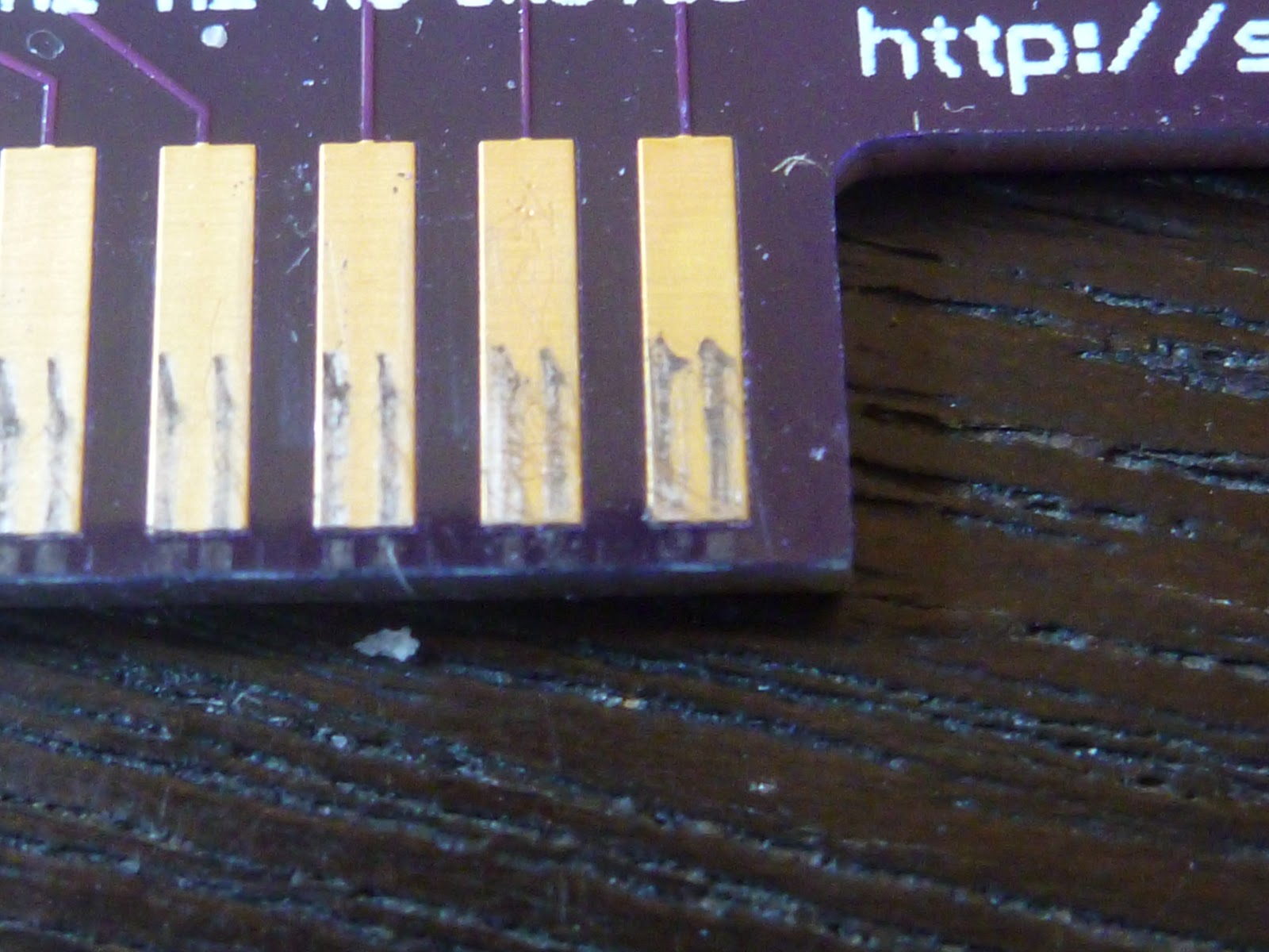
Prompted by a question about the durability of board when faced with multiple insertions and removals into the edge connector, I decided to run a little test. I took one of the spare ALU boards (made by Dorkbot PDX) and one of the edge connectors I got from Jameco, and did 100 insertions. I took measurements after each batch of 10 insertions and removals. I didn't take pictures as I went, but I did take pictures at the end.
There was minor abrasion visible on the card edge after 10 cycles. Nothing alarming by any means, but you could see it if you tilted the board to the light just right. The abrasion got progressively more visible as the cycles continued; they're very visible at 100. I characterized the abrasion by measuring resistance. I figured if it got too bad, I'd see increased resistance. I took measurements in two places: First, from one end of the card edge pad to the other, and second from the card edge to the corresponding output pin on the edge connector.
There wasn't any noticeable change for the first 80 cycles. I'd consistently see about 0.4-0.5 ohms on the pad, and about 0.6 ohms from pad to pin. At the 90 cycle mark, I saw 1 ohm on the pad, and 2.2 ohms on from pad to pin. The 100 cycle test saw the edge connector resistance increase to 2.3 ohms. I took the measurements with my Extech EX330, using the stock pen-type probes.
Here are pictures of the board after 100 cycles. I made a point of inserting the card into the connector the same way each time. The side with the heavy abrasions went into the connector first, so I guess it had the insertion as well as some amount of rotation when I put the other end of the card in.
I went at one of the pins with a hobby knife, and what I found underneath the gold(?) coating matched the abrasions. I'm assuming what that means is that the abrasions are the result of the coating being rubbed off, rather than some sort of transfer from the edge connectors.
The signals I'm sending across these edge connectors aren't terribly sensitive, so I'm guessing I needn't lose any sleep over the increase in resistance that comes from repeated insertion/removal cycles. If I do start to care (or need to care), it looks like I can reduce the impact of those cycles by pushing the board straight in, rather than one corner at a time. That'll increase the force on the board that's holding the edge connector, though. So many tradeoffs...
Is there anything more exciting than running off the edge of a breadboard and realizing that your OCD won't let you put in long jumper wires -- that you're going to have to rip the whole thing up, shift it over a bit, and rewire it all again?
I think the ALU is finally done, and ready for PCB manufacture.
Of course, now that I've said that, something will go horribly wrong (but let's pretend it won't).
Specs:
8-bit ripple-carry
Supports addition, subtraction, AND, OR, and NOT
Exports Zero, Negative, Overflow, and Carry condition codes
41 7400-series logic chips:
21 Quad NAND (7400)
2 Quad NOR (7402)
2 Hex NOT (7404)
4 Dual 4-1 Mux (74153)
7 Quad 2-1 Mux (74157)
2 Quad Buffer (74125)
3 Octal Buffer (74541)
All the processing power (actually less) of a pair of 74183s, at several times the cost!
Here's a picture:
The blindingly-white breadboard on the left is the core of the ALU. The buffer chips live on the middle breadboard. The PCB on the right is the Front Panel I described earlier. Briefly, the Front Panel allows me to control the ALU from my computer. First, this allows me to implement the UI in software rather than switches and LEDs. Second, I can perform automated regression tests by simply running a script.
With the exception of the rainbow-colored ribbon cables, I wired the entire circuit in red and black. Why? I was told that blue and yellow wires are slower than red and black ones. Or Radio Shack only stocks red and black in the big rolls. You choose.
The ribbon cables are Adafruit "Premium" Jumper Wires electrical-taped together. I really wanted an 8-conductor cable, but Adafruit only carries 6-conductor cables (six???). The only other choice seemed to be ordering housings, crimp terminals, and wire separately from Mouser and building them myself. Compared to that, taping together cables seemed easier (not to mention cheaper).
Everyone loves video, so here's a video. It's a flyover of the breadboarded circuit followed by a wonderfully-shaky look at the GUI I use to control the ALU interactively.
Now to the guts of the circuit. First, the schematic:
Next, the board layout. It's easily the most complicated board I've designed (n=2), and it just barely fits in the routing space allowed by Eagle Hobbyist. Unless I'd been willing to cut the circuit in half (or maybe smaller), I quite simply wouldn't have been able to do it in free Eagle. Had space not been so tight, I might've (ok, would've) ditched the buffer chips in favor of back-to-back NOTs. Maybe if I get really really bored, I'll make daughterboards which plug into the buffer sockets and use NOTs to implement the buffers.
The first page shows the board layout without the back-side ground fill. The second page shows the fill (the individual wires are a mite difficult to see through the rivers of purple).
Just routing this board was an adventure. When I first laid it out, I naively let the autorouter do the whole thing. It routed every trace, which was great, but it picked some mindbendingly roundabout paths for some of the signals. I knew I'd go insane if I tried to route the whole thing, so instead I hand-routed the traces I cared about (primarily the A0-7, B0-7, R0-7, and control lines) and let the auto-router take care of the rest. Eagle doesn't seem to go quite so crazy when you only give it short wires to route. Unfortunately, it wasn't able to route the entire board -- there's one signal left, so I'll have to solder a jumper wire to complete the circuit.
When I made the Front Panel, I was a little conservative with the silkscreening. This time, I went in the other direction. Waaaay too far in the other direction. I added silkscreen labels to everything that wasn't moving, and also labeled some things that were just moving slowly. The chips that calculate the individual bits are labeled. The control bits are labeled. The pads on the edge connector are labeled. Every IC has a label which will be (gasp) still visible when the socket is installed (I learned this the hard way with the Front Panel). I'm sure there's something I forgot to label, but I should be in much better shape with this board.
At the suggestion of a coworker, I made some space in the bottom right of the board for a single 16-pin DIP just in case. Just in case what, I don't know yet, but I'm sure it'll be nice to have a place to put a chip if I need it.
Why is there an edge connector on the board? This board will be but one component of my microprocessor. The control logic will live on a backplane board, and individual subsystem boards will plug into it via ISA sockets. I'm not using the ISA bus -- just the physical sockets. There won't be any bus at all, as a matter of fact. I'm simply breaking the microprocessor up into several boards so that a) I can develop them separately and b) I can work with them in Eagle without having to shell out $1600 for the professional version.
Lessons Learned
The Front Panel as originally designed has 27 output pins (numbered 0-26) and 8 input pins (numbered 100-107). Output pins 0-23 use 74595 serial-to-parallel latches (which are in turn connected to the Front Panel's microcontroller), while pins 24-26 are connected directly to the microcontroller. Input pins 100-107 connect to the microcontroller via a 74165 parallel-to-serial latch. This configuration worked when I was testing ALU bits 0-7, but came up short when I added the four condition codes (zero, negative, overflow, and carry). Negative is the same as R7, so I needed to find three extra input pins.
I solved that problem by changing the Front Panel software to allow pins 24-26 to function as input pins (numbered 124-126) on demand. Very happy with myself for coming up with this solution, I wired the whole thing up and watched as my current consumption skyrocketed from a normal 20mA to 120mA. Some very exciting(?) debugging ensued. It turns out that the newly-minted input pins 124-126 sink about 30mA each. Maybe I don't have them configured correctly in the microcontroller -- who knows. Bottom line, they were sinking power in a way pins 100-107 weren't. They differ from 100-107 in that 124-126 carry condition codes, which means the weird power behavior only exhibited itself when those codes were active, and of course the power consumption changed depending on how many were active. Only condition code zero? +30mA. Zero, Overflow, and Carry? +90mA. Very exciting. Eventually I figured out what was happening, added some series resistors, and all is well. I need to double-check that I'm initializing the pins correctly in the Front Panel microcontroller, as it's possible the microcontroller could take care of this for me, ridding me of the need to use the series resistors.
I also learned, the hard way, that thou shalt always ground thy unused inputs. I don't have many unused gates in this design (3 NAND, 3 NOR, and 4 NOT), but I had initially left their inputs floating. I was seeing some truly bizarre behavior from the chips containing those unused gates. I haven't tried to reproduce since then, but I swear the unused gates were influencing the output of the active ones. That is, use gate A on a 7400, leave B-D floating, and watch A behave very strangely. I'm far too burned out on this circuit at the moment to go investigate further, but I think that's what I saw. Anyway, I haven't seen anymore weirdness since I grounded the inputs for every unused gate.
Labels and diagrams are very important. Every ribbon cable now has a label on it which says which wires are which signals. Almost every IC has a sticker on it with its U number. I even created a map of the breadboard in Inkscape which shows the position of every IC and the signals for every header pin. These diagrams saved much time.
Next Steps
Now that I have the circuit working in breadboarded form, I'm going to have PCBs made by DorkbotPDX. They did an awesome job with the Front Panel, so I'm very happy to have them make this board too. I had to use 6mil traces for everything (except power), so hopefully that'll turn out OK. Once the PCBs come in, I'll populate one, test it out, and then gleefully reclaim my breadboards. The ALU has consumed almost all of my breadboard space, leaving me with one dinky Radio Shack 63-row breadboard to play with. It'll be nice to have the big breadboard back.
Once I'm satisfied with the ALU, I think it'll be time to tackle the register file. Perhaps I should start designing it. I also have to think about the control circuitry for the whole processor, what the instruction set will look like, and all that. While I had initially planned to implement the microprocessor in CODE, I may have decided to just do my own thing instead. We'll see.
A friend asked how many boards I'd get from Dorkbot (3), and promptly suggested that I could populate all of them, chain them together, and get a 24-bit adder. Then I could build a 24-bit machine! Um, no. Eight bits is enough for me until I work on microprocessor v2, which will be done with a CPLD. Well, eight bits is enough for me for the datapath. The address path will be at least 24 bits, if not 32. But that's a story for another day.
Last but not least
Here's the output from the verifier running its regression tests over the breadboarded ALU. It's music to my ... eyes.
Testing ADD
ADD case 1/7
ADD case 2/7
ADD case 3/7
ADD case 4/7
ADD case 5/7
ADD case 6/7
ADD case 7/7
Testing SUB
SUB case 1/7
SUB case 2/7
SUB case 3/7
SUB case 4/7
SUB case 5/7
SUB case 6/7
SUB case 7/7
Testing NOT
NOT case 1/3
NOT case 2/3
NOT case 3/3
Testing OR
OR case 1/9
OR case 2/9
OR case 3/9
OR case 4/9
OR case 5/9
OR case 6/9
OR case 7/9
OR case 8/9
OR case 9/9
Testing AND
AND case 1/9
AND case 2/9
AND case 3/9
AND case 4/9
AND case 5/9
AND case 6/9
AND case 7/9
AND case 8/9
AND case 9/9
Success