Digression: The ICM7212 controls four 7-segment displays. The 40-pin DIP has one pin for each segment on each display, four digit pins, and four data pins. To display a value on a given 7-segment display set the data lines with the desired value, and toggle the appropriate digit line. This circuit will have eight data lines inbound, so we'd need a quad 2-1 mux (the 74HCT157, for example). We only need to toggle two digit lines, which we could do with a 555 and an RTL inverter.
For giggles, let's cost it out (all prices from mouser.com for individual quantities); $6.70 for the ICM7212, $0.47 for the timer, and $0.69 for the mux. We'll assume that the resistors, capactors, and transistors needed for the 555 timer glue and for the inverter are free. $8.55 for the whole thing. Oh, and the ICM7212 is huge.
All of this is a long way of justifying doing it with a microcontroller instead. The added advantage of doing it with the microcontroller and shift registers is that I'll likely see them again (and again and again), so it'd be helpful to gain some experience.
So the current plan is to do something with an ATtiny85 microcontroller. A parallel-in-serial-out (PISO) shift register on the input, sampled periodically by the microcontroller, and two serial-in-parallel-out (SIPO) shift registers on the output. If we can share the clock lines between all three chips, I think we can get away with using only four pins on the microcontroller. The tiny has 6, excluding VCC and GND, so this should be doable.
To familiarize myself with the chips required, I decided to build the beAVR setup described here. It's nothing fancy -- just an ATmega644 with supporting gunk (caps, clock, etc). I don't have the USB-to-5V serial cable recommended in the article, so I also had to add an SP3232EBCP RS232 transceiver so I could hook up the USB serial line. This won't be needed for the final design, with the tiny, but it's nice to have for debugging. Who knows -- with two pins left, maybe I can use it on the tiny.
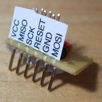
I've done the medusa head AVRISP2 connection before. I didn't like it then, and I don't like it now, so this time I decided to do something about it. I built a little breakout board that transforms the 2x3 pin ISP connector to 1x6pin, which is compatible with the breadboard. Here are some pictures:
Things I learned from building this thing:
- The Helping Hands are amazingly useful. Now I have a stable suspended platform on which to solder. It makes things like header pin alignment considerably easier.
- The default font in TextEdit (12pt Helvetica?) has precisely the right vertical spacing when you print at 50%.
- To attach the labels, print on a full-size sheet of paper, cut out the width to fit (from the top of the VCC to the bottom of the MOSI), but leave it an inch or two longer than necessary. This gives you a nice handle with which to hold the label while you superglue it to the plastic thing on the header.
- I'm not a huge fan of long pad-to-pad solder bridges. I like wires. They're much less fussy than bridges.
- Hot glue is, once again, my friend. I used it to protect the underside of the PCB.
What I'll do differently next time (there will be a version two):
- This version's pin mapping between the 2x3 header and the 1x6 is based on shortest distance. Unfortunately, that approach results in a 1x6 ordering that doesn't match the pin ordering on the ATmega644. As I'll likely be doing most of my programming with the mega, I'd rather the breakout board just drop into place, without requiring me to string wires hither and yon. Version 2's mapping will follow the ATmega644 pin ordering. VCC and GND may be shifted back on the board, behind the 2x3, allowing them to plug directly into the breadboard power rails.
- Pin labels should be visible regardless of breakout board orientation. In this version, they're only visible from the front, which makes it awkward when I install it with the front facing away from me. The paper is fragile, but I knew that going in. We'll see how it works out. I may need to switch to another material.


No comments:
Post a Comment